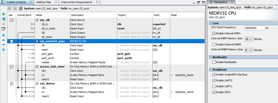
NEORV32 Test Setup using the NEORV32 as a Nios II drop-in replacement
This setup provides a very simple "demo setup" that uses the NEORV32 Qsys/Platform Designer component so that the NEORV32 can be used as a drop-in replacement of the Nios II soft CPU from Intel. The demo is running on the Terasic DE0-Nano FPGA Board.
The design is based on the de0-nano-test-setup, but the NEORV32 cpu is added as a QSys/Platform Designer component. As an example the DMEM is "external" and uses an Platform Designer SRAM block.
For details about the design and use of the NEORV32 as a Qsys/Platform Designer component please
look at the Qsys component files and documentation here NEORV32 Qsys Component
It uses the simplified simple example top entity that provides a minimalistic interface (clock, reset, UART and 8 LEDs).
- FPGA Board: 📚 Terasic DE0-Nano FPGA Board
- FPGA: Intel Cyclone-IV
EP4CE22F17C6N - Toolchain: Intel Quartus Prime (tested with Quartus Prime 18.1.1 - Lite Edition)
NEORV32 Configuration
For NEORV32 configuration the default values of the neorv32_top in version 1.6.0 are used with a few exceptions:
- Memory: 16kB instruction memory (internal IMEM), 8kB data memory (external DMEM), No bootloader
- Tested with version
1.6.0 - Clock: 50MHz from on-board oscillator
- Reset: via on-board button "KEY0"
- GPIO output port
gpio_o(8-bit) connected to the 8 green user LEDs ("LED7" - "LED0") - UART0 signals
uart0_txd_oanduart0_rxd_iare connected to the 40-pin GPIO_0 headeruart0_txd_o:output, connected to FPGA pinC3- header pinGPIO_01(pin number "4")uart0_rxd_i:input, connected to FPGA pinA3- header pinGPIO_03(pin number "6")
FPGA Utilization
Total logic elements 4,064 / 22,320 ( 18 % )
Total registers      1932
Total pins           12 / 154 ( 8 % )
Total virtual pins   0
Total memory bits    230,400 / 608,256 ( 38 % )
Embedded Multiplier  9-bit elements	0 / 132 ( 0 % )
Total PLLs           0 / 4 ( 0 % )
How To Run
Open the Quartus project file, compile and upload to FPGA.
